
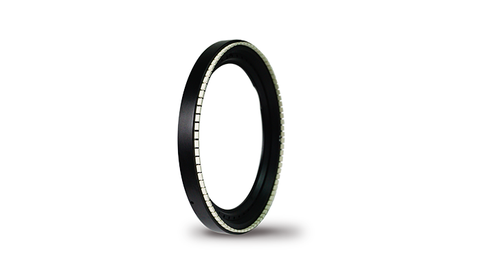
Application Scenarios
Manufactured with a vitrified bond that is heat-resistant,wear-resistant, and offers excellent heat dissipation-preventing micro-cracks and thermal damage, TTV less than or equal to 3 μm,damaged layer depth less than 2.7 μm and exceptional efficiency can be achieved.. The product brings positive effect, namely foreign monopoly can be broken and customers costs reduce.
1.Extremely high hardness, usinghigh-sharpness0diamond for high grinding efficiency
2.Designed for very brittle materials - high wheel sharpness reduces surface damage and stress
3.Superior heat dissipation, avoiding thermal damage
4.Stable self-sharpening - no passivation, no wheelclogging, consistent processing quality
Model Specifications
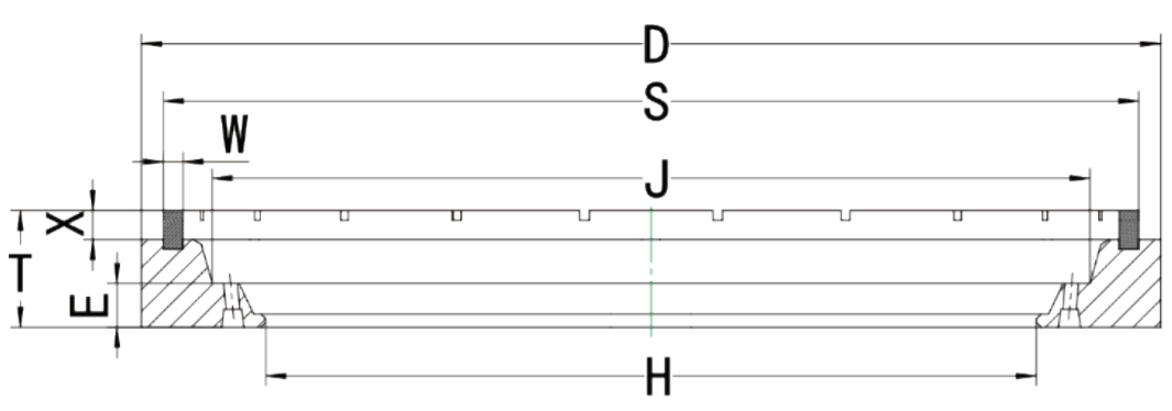
6A2T
Model | D | T | H | X | W | Bond | Grit Size |
| 6A2T | 209 254 313 | 30 | 95 155 158 237 | 5 7 | 2 3 4.5 4 | B | 325 2000 |
Workpiece | GaN Wafer |
Workpiece Size | 4-Inch |
Wheel Specification | 6A2T D209 (8 In) V 2000 |
G-Ratio(Wheel wear : Workoiece removal) | 1:3 |
TTV | ≤3μm |