
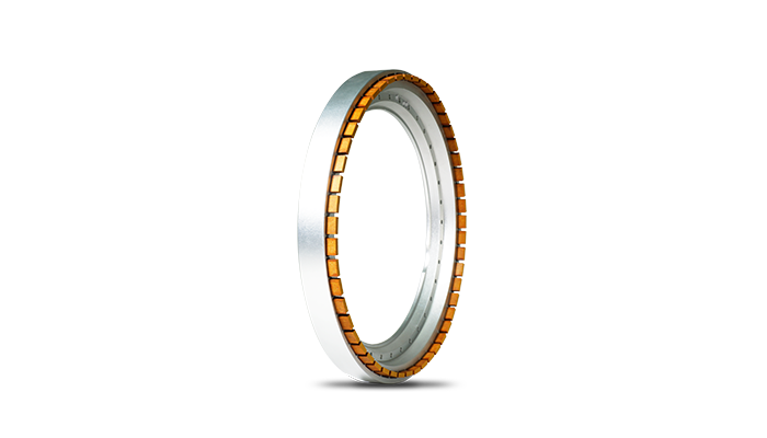
Application Scenarios
Resin bond is chosen, with gentle grinding force and a roughness of Ra≤10nm. Customized specifications are avail-able, suitable for small-batch high-precision processing,and compatible with precision thinning equipment. The precision and efficiency reach leading level of the industry.
1.Good toughness and excellent surface quality
2.High sharpness, low stress, and low subsurface damage
3.Excellent self-sharpening, easy chip evacuation - no chip adhesion or wheel clogging
Model Specifications
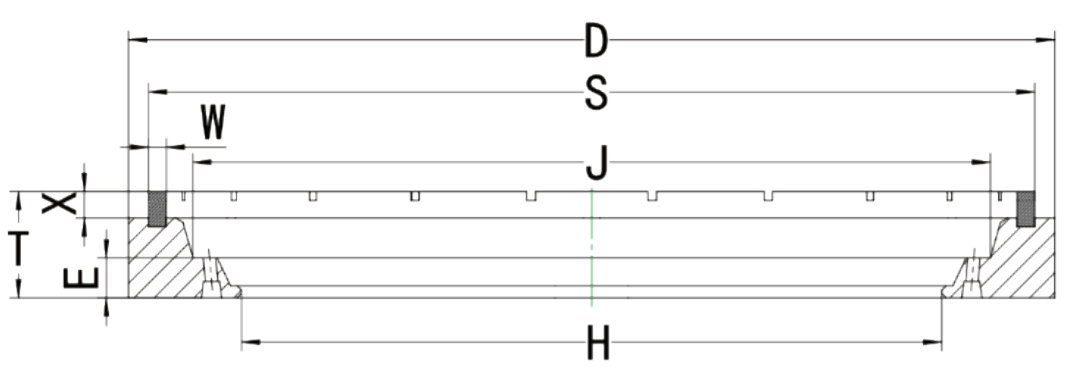
6A2T
Model | D | T | H | X | W | Bond | Grit Size |
6A2T | 209 254 313 | 30 | 95 155 158 237 | 5 7 | 2 3 4.5 4 | B | 600 2000 |
Workpiece | GaAs Wafer | |
Workpiece Size | 6 Inch | |
Wheel Specification | 6A2T D209 (8 In) B 600 | 6A2T D209 (8 In) B 2000 |
Surface Quality | Uniform grinding marks | High gloss, uniform marks no deep scratches |
Roughness | - | ≤10nm |
TTV | ≤3μm | ≤3μm |