
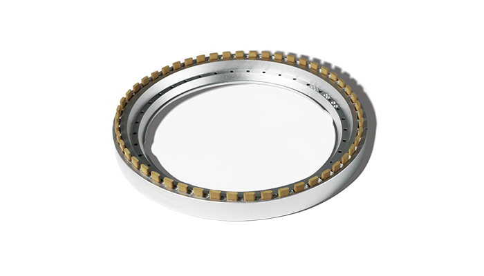
Application Scenarios
Vitrified/resin bond utilized, suitable for IC packaging process; surface roughness Ra < 2 nm, TTV s 3 μm. Alumi-num alloy substrate with high thermal conductivity and corrosion resistance.Rotational speed: 1000-3500 r/min, feed rate: 1.0-1.4 μm/s, compatible with mainstream equipment.
1.Ultra-high speed, high stock removal
2. Extremely low subsurface damage (SSD)
3.High flatness, low TTV
4.Strong self-sharpening, no passivation
5.Ultra-light grinding force, low stress
6.Zero metallic contamination
Model Specifications
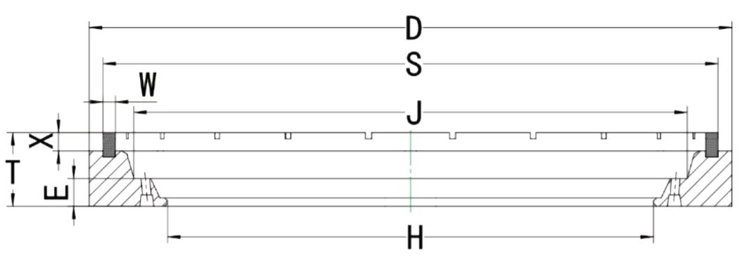
6A2T
Model | D | T | H | X | W | Bond | Grit Size |
6A2T | 209 254 313 | 30 | 95 155 158 237 | 5 7 | 2 3 4.5 4 | B V | 325 2000 30000 60000 |
Workpiece | Si Wafer |
Workpiece Size | 12 inch |
| Wheel Specification | 6A2T D313 (12 in) V 60000 |
| Surface Quality | Uniform grinding marks |
| Roughness | ≤2nm |
| TTV | ≤2μm |
| Warp | ≤10μm |
| Bowl | ≤2μm |