
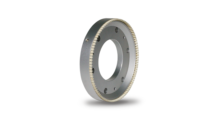
Application Scenarios
The double-sided thinning of wheels for semiconductor silicon wafers is specially designed for the precise double-sided grinding of wafers, with high flatness, low damage, low contamination, long service life, and stable grinding performance. It is used to achieve high-precision thickness control, parallelism control, and low-dam-age surface processing of silicon wafers.
1. Ultra high thickness uniformity & flatness
2. Low subsurface damage
3.Zero metallic contamination
4.Excellent self sharpening & stable grinding force
5.Good cooling & chip evacuation
6.Low wear, long service life
Model Specifications
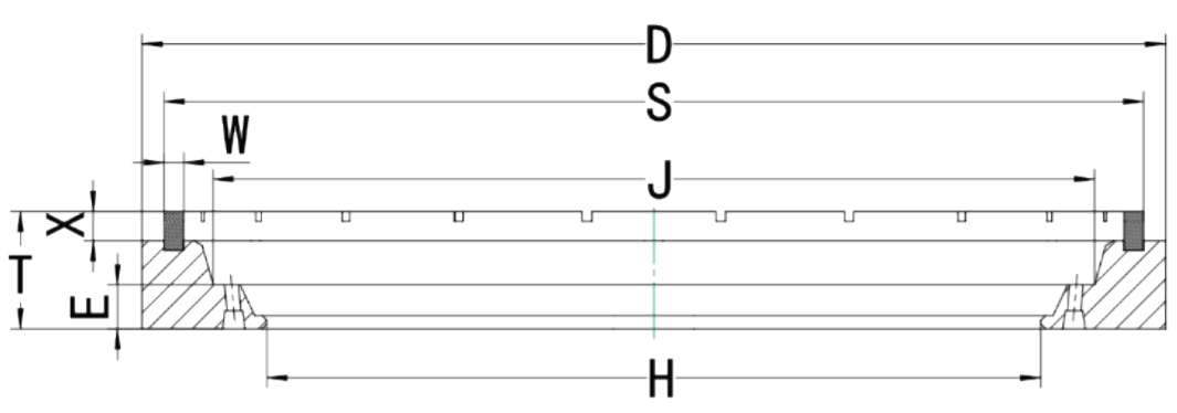
6A2C
Model | D | T | H | X | W | Bond | Grit Size |
6A2C | 160 | 25 | 80 | 5 | 5 | V | 3000 |
Workpiece | Silicon Wafer (Double-sided removal respectively :42.5um) |
Workpiece Size | 12 inch |
Wheel Specification | 6A2C D160 V 3000 |
G-Ratio(Wheel wear : Workoiece removal) | 1:28 |
Roughness | The surface is uniform without deep lines |
TTV | ≤0.5μm |
Warp | ≤10μm |
Bowl | ≤2μm |